Below are some pictures of the chips we have designed in
the past (click on the miniature for a bigger picture). The brief
descriptions also contain links to some older project pages, please click to explore!


![]()
|
| Projects | Chip Gallery | People | Publications | PhD Study | Contact |
Chip Gallery
Below are some pictures of the chips we have designed in
the past (click on the miniature for a bigger picture). The brief
descriptions also contain links to some older project pages, please click to explore!
|
|
|
|
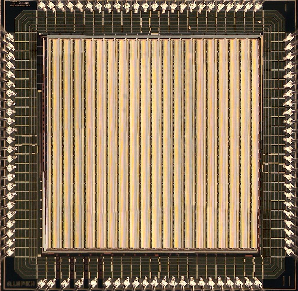
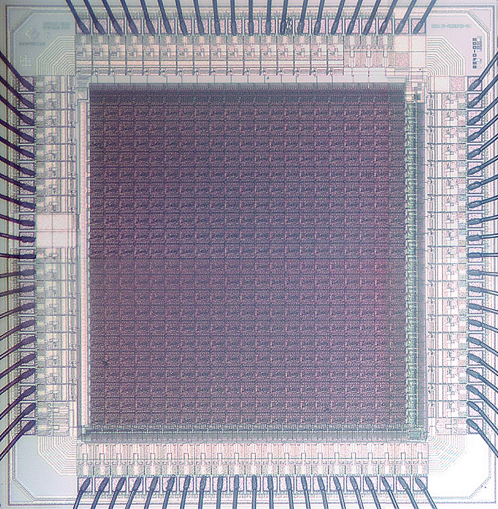
ASPA-3 (2009) The latest chip from the ASPA family, with 160x80
processor array into 50mm2 of silicon, with improved
performance. |
|
|
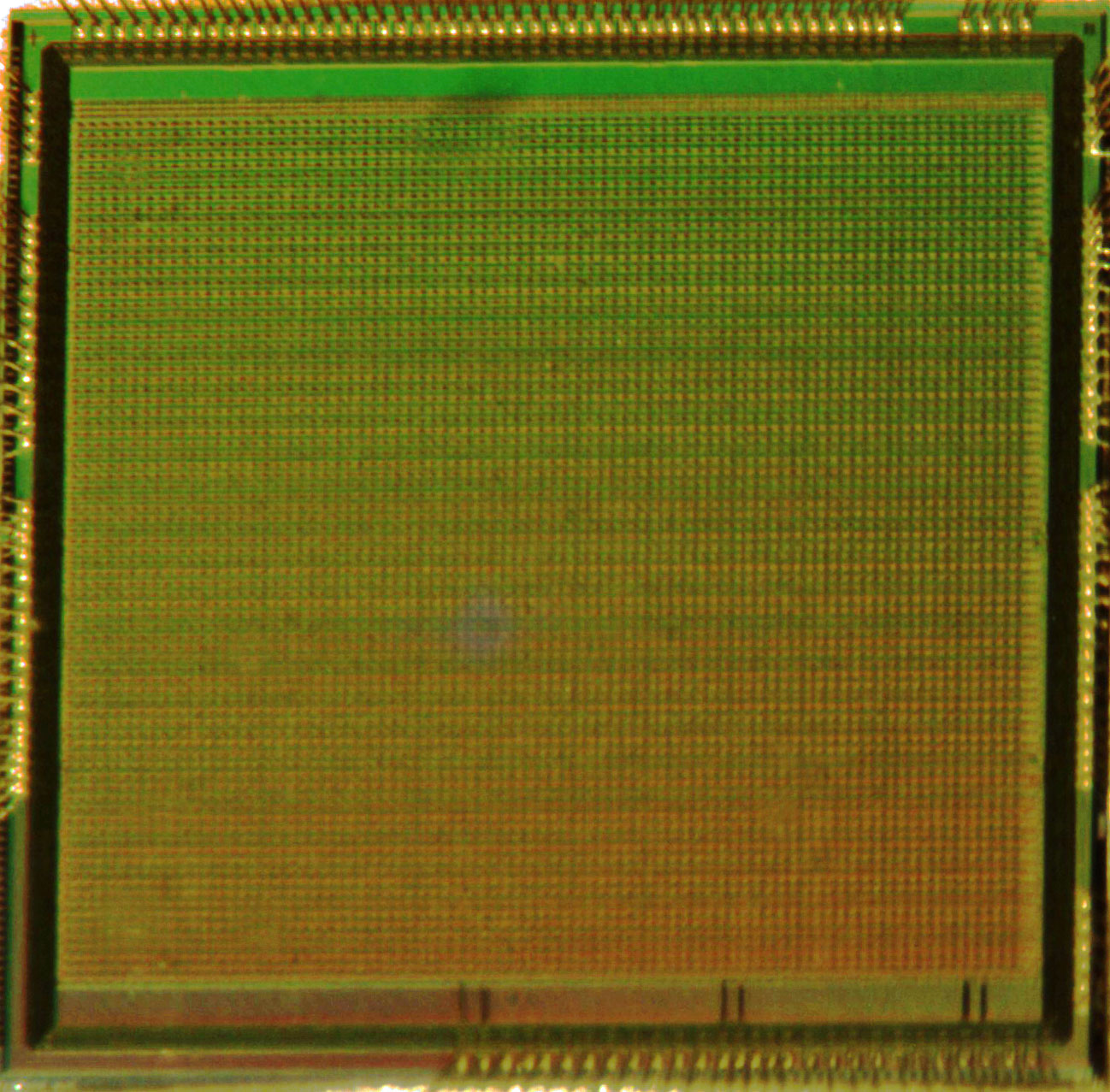
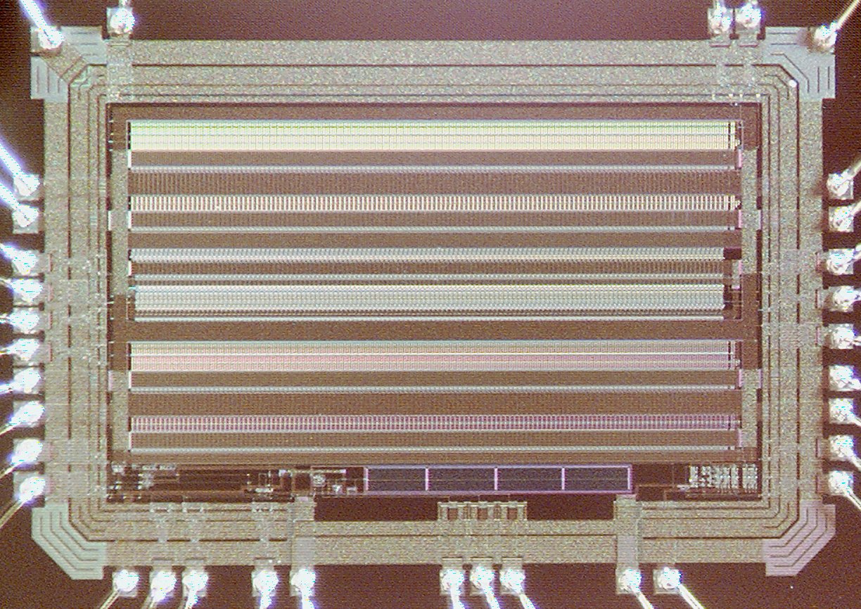
ASPA-2 (2008) The second generation ASPA chip is designed in a 180nm
CMOS technology. It contains 80x80 processor array, with synchronous SIMD
and asynchronous wave-propagating mode. Peripherial circuits perform
coordinate address extraction for efficient object localisation and
tracking |
|
|
SpikeNeuron
(2007). This chip contains
200 analogue neuron cells. Each cell mimics spiking and bursting firing
behaviour of cortical neurons, producing biologically plausible spike shape,
is programmable so that various neuron types can be modelled, and does so
with a remarkable efficiency of only 8pJ/spike. |
|
|
ASPA
(2007). This general-purpose
vision chip which uses digital processing elements with a
mixed bit-serial/8-bit architecture and asynchronous/synchronous control. It
is particularly efficient at executing image processing operations that
involve wave-propagating algorithms, such as reconstruction, skeletonisation,
watershed segmentation, etc. more... |
|
|
ACLA
(2007). This is a prototype
design of the Asynchronous Cellular Logic Array. The chip demonstrated binary
wave propagation at speed of below 0.5ns/pixel at energy consumption of
0.4pJ/pixel. The circuitry has has been subsequently included in the ASPA
processor array chip. |
|
|
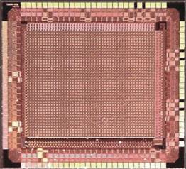
SCAMP-3
(2005). General-purpose programmable
vision chip with a 128x128 SIMD
processor-per-pixel array fabricated in a 0.35um
CMOS technology.The chip is capable of 20 GOPS at 250mW power,
while many image processing algorithms run
at 20fps with a few mW of power!
more... |
|
|
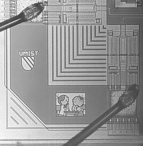
Bolek
i Lolek (2003). This chip
contained various test circuits and prototypes of analogue signal
processing cells, including gas sensor interface, novel switched-current error
correction circuitry and chaos generator
cells. It also contains a nice piece of 'chip art' - the cartoon is just
100um wide! |
|
|
SCAMP-2
(2003). This chip was a
scaled and improved version of the SCAMP vision chip, and served as a
prototype for the SCAMP-3 device. The general-purpose
programmable vision chip contains a 39x48 SIMD
processor-per-pixel array fabricated in a
0.35um CMOS technology. Flexible readout architecture
enables global operations. |
|
|
SCAMP-1
(1999). This was the first SCAMP (SIMD Current-mode Analogue Matrix Processor)
chip. This
10mm2 integrated circuit was a proof of concept of
the SCAMP approach, integrating image sensing and a 21x21 array of
pixel-parallel analogue processing elements. |
|
|
Gepanapa
(1998). This is a prototype chip that contains 15 general-purpose
"analogue microprocessors".
These processors execute software programs, in a way akin to a digital
microprocessor, while operating on analogue data samples,
achieving excellent performance/power and performance/area ratios.
This work led to the development of SCAMP vision
chips. |
|
|
VDL
TDC (1997). A high resolution time-to-digital converter utilising a
Vernier
Delay Line concept. The integrated circuit that was fabricated in 0.7um
digital CMOS technology. The TDC provides time measurements
with resolutions in a range of 30ps to 250ps
(stabilised using a DLL) or as high as 5 ps (with
external biasing and calibration) |
|
|
|