|
| Projects | Chip Gallery | People | Publications | PhD Study | Contact |
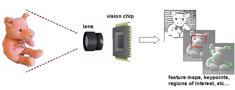
The SCAMP Vision Sensor integrates a massively parallel SIMD processor array into the pixels of the image sensor device. Unlike a conventional image sensor, it does not output raw images, but rather the results of on-sensor computations, for instance a feature map, optic flow map and/or address-events describing locations of pixels of interest. The device is fully programmable, to execute a variety of vision algorithms. As early vision computations are done entirely on-sensor, high speed and low-power consumption of the entire camera system is obtained, enabling new embedded vision applications in areas such as robotics, industrial machine vision, remote monitoring, wearables, VR, toys, etc.
On this page, you can find out more about the SCAMP-5 vision chip architecture and implementation, the smart camera development kit based on this device, and see the demonstrations of various algorithms implemented on the device.
In a conventional machine vision system, images are acquired, digitised, and transmitted off camera, frame after frame. The processor system then needs to keep up with the resulting pixel avalanche, with large amount of data continually exchanged between the sensor, processors and the memory, to implement required vision algorithms. This is inefficient. Our approach, inspired by the biology, is based on moving the computation from the processor system to the sensor itself. Essentially, we embed a parallel processor array into the image sensor. The approach has a number of advantages:
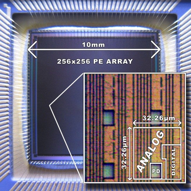
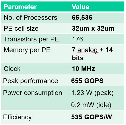
The SCAMP-5 vision chip contains a 256x256 processor array, operating in a SIMD mode, with one processing element per image pixel. The processors are simple albeit fully software-programmable entities, comprising local memory, ALU, control and I/O circuits. Mixed-mode datapath allows the execution of some operations in the analog domain, achieving low-power and bypassing the need for A/D conversion. The results of computation can be read-out as grayscale images (mostly for debugging purposes) and binary images. If the results of computations are sparse (e.g. when points of interest are identified), an address-event read-out allows to minimise the bandwidth between the sensor chip and the rest of the system.
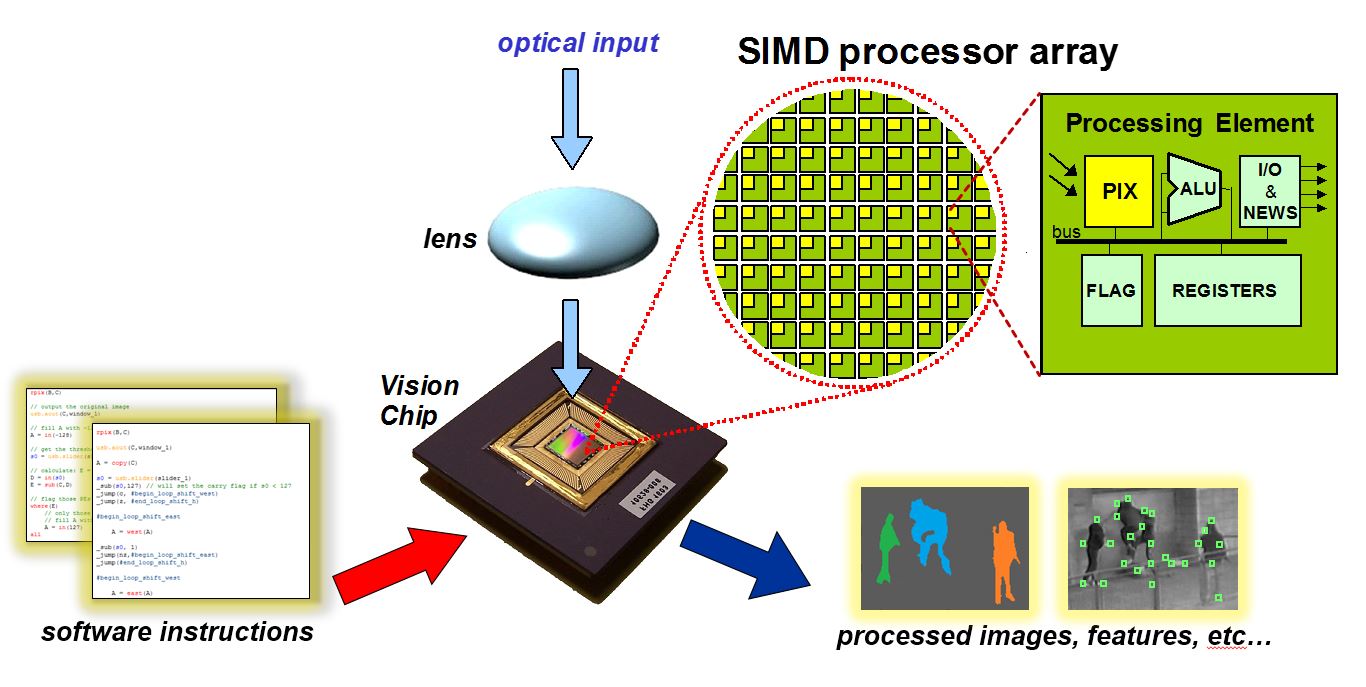
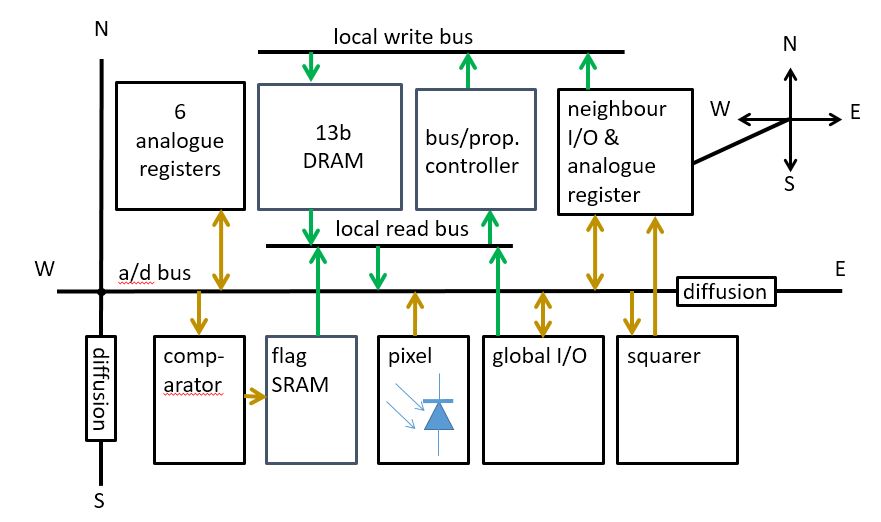
Each of the 65,536 processors contains six analog registers (capable of storing a real-valued variable, e.g. a gray-level pixel value), 13 bits digital memory, and circuits for performing arithmetic and logic operations on the local data, as well as neighbourhood operations. It also contains hardware accelerators for asynchronous binary flood-fill and spatial gray-scale low-pass filters, as well as control and I/O circuits. The processing elements execute instructions broadcast to the entire array from a common controller, with local autonomy provided via an ativity flag. The photosensor circuit is tightly coupled to the processor.
The chip is a custom mixed-mode integrated circuit implemented in 180nm CMOS technology. It can carry out over 500 GOPS (billion operations per second) at power consumption below 1W. We have demonstrated processing speeds up to 100,000 fps (frames per second), although a typical high-speed operation in a robotic application may be at 1000s fps or less. The power depends on the processing load, i.e. the algorithm and frame rate, and can be below 1 mW for simple low frame-rate operations.
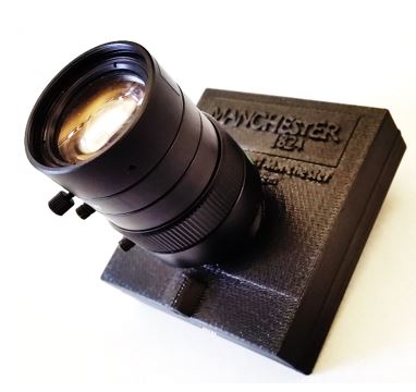
We have integrated the SCAMP chip into a reference smart camera design, and have provided software tools that allow the development of SCAMP algorithms for various applications. The SCAMP camera includes a USB interface for development, as well as SPI and GPI/O interfaces for embedded applications. It also includes an application processor (Cortex-M4) an inertial measurement unit (IMU) for custom applications.
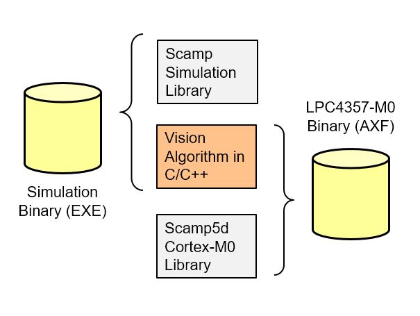
The chip is programmed using a C based program flow, using provided libraries that allow parallel processing kernels to be executed on the processor array. The SCAMP processor emulator, running on a PC (Windows), allows debugging of the programs that will be executed on the SCAMP chip. The SCAMP kernel code can be stepped-through, with full insight into the contents of all registers on the device.
More details, and software downloads can be found in the online SCAMP System Documentation.

High-speed eye tracking, up to 10kHz, 0.1 ms latency.
L.Bose, J.Chen, S.Carey and P.Dudek, "Pixel Processor Arrays For Low Latency Gaze Estimation", IEEE Conference on Virtual Reality and 3D User Interfaces, IEEVR 2022, pp 970-971, March 2022


Object recognition, gesture recognition, etc. running entirely inside the camera
H.M.So, L.Bose, P.Dudek, G.Wetzstein, "PixelRNN: In-pixel Recurrent Neural Networks for End-to-end-optimized Perception with Neural Sensors", IEEE/CVF Conference on Computer Vision and Pattern Recognition, CVPR 2024, pp.25233-25244, June 2024 [website]
Y.Liu, L.Bose, J.Chen, S.J.Carey, P.Dudek, W.Mayol-Cuevas, "High-speed Light-weight CNN Inference via Strided Convolutions on a Pixel Processor Array", British Machine Vision Conference, BMVC 2020, paper 126, p.1-14, September 2020
L.Bose, P.Dudek, J.Chen, S.J.Carey, W.Mayol-Cuevas, "Fully embedding fast convolutional networks on pixel processor arrays", European Conference on Computer Vision, ECCV 2020, pp.488-503, August 2020 [video]
L.Bose, J.Chen, S.J.Carey, P.Dudek and W.Mayol-Cuevas, "A Camera That CNNs: Towards Embedded Neural Networks on Pixel Processor Arrays", Proceedings of the IEEE International Conference on Computer Vision, ICCV 2019, Seoul, pp.1335-1344, October 2019
![]()
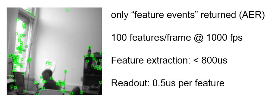
On-sensor feature extraction, keypoint selection, and tracking. Applications in motion estimation, visual odometry, SLAM. Up to 3000 fps (when returning only keypoint coordinates / descriptors).
L.Bose, J.Chen and P.Dudek, "Descriptor-In-Pixel : Point-Feature Tracking For Pixel Processor Arrays", IEEE/CVF Conference on Computer Vision and Pattern Recognition, CVPR 2025, pp.5392-5400, June 2025. [website]


People counting, loiterer detection, security etc (all analysis done on-sensor, at low power, no need to transfer images/video to the could)
 (Martel et al. 2016)
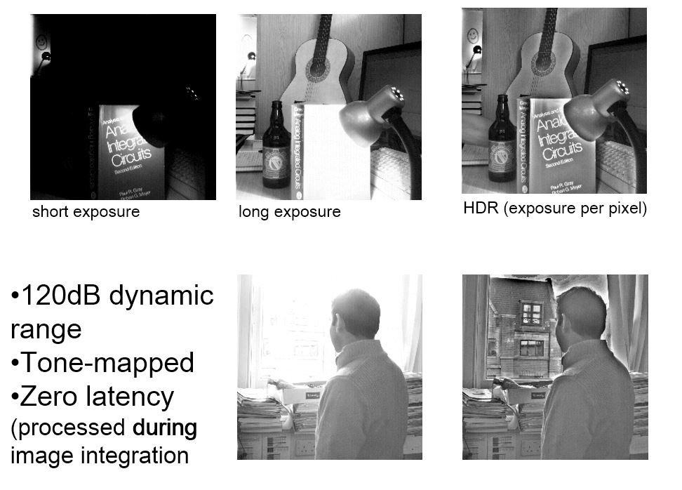
H.M.So, J.N.P.Martel, P.Dudek, G.Wetzstein, "MantissaCam: Learning Snapshot High-dynamic-range Imaging with Perceptually-based In-pixel Irradiance Encoding", International Conference on Computational Photography, ICCP 2022, August 2022
J.N.P.Martel, L.K.Muller, S.J.Carey and P.Dudek, "Parallel HDR tone mapping and auto-focus on a cellular processor array vision chip", IEEE International Symposium on Circuits and Systems, ISCAS 2016, Montreal, pp.1430-1433, May 2016


High-speed reconstruction: (left) encoded image, (right) reconstructed video (Martel et.al. 2020)
480 fps videos reconstructed from 30 fps coded exposure image frames. Only the encoded frame is transmitted of sensor. The encoder & decoder are end-to-end trained, see Neural Sensors page for more details.
J.N.P.Martel et.al. "Neural Sensors: Learning Pixel Exposures for HDR Imaging and Video Compressive Sensing with Programmable Sensors", IEEE Transactions on Pattern Analysis and Machine Intelligence, Volume 42, Issue 7, pp. 1642-1653, July 2020 [website]


Block matching motion estimation. 5x5 block search, 5x5 range, up to 2000 frames per second.
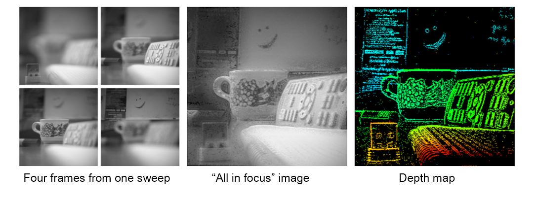
Monocular depth from focus, 128 depth levels at 60 fps, using a liquid lens
(Martel et al. 2018)
J.N.P.Martel, L.K.Muller, S.J.Carey, J.Muller, Y.Sandamirskaya and P.Dudek "Real-Time Depth From Focus on a Programmable Focal Plane Processor", in IEEE Transactions on Circuits and Systems I: Regular Papers, vol 65, no.3, pp. 925-934, March 2018
J.Chen, S.J.Carey and P.Dudek, "Feature Extraction using a Portable Vision System", IEEE/RSJ International Conference on Intelligent Robots and Systems, Workshop on ision-based Agile Autonomous Navigation of UAVs, IROS 2017, September 2017
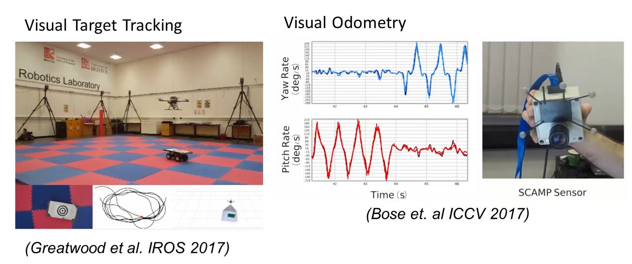
C.Greatwood, L.Bose, T.Richardson, W.Mayol-Cuevas, J.Chen, S.J.Carey and P.Dudek, "Tracking control of a UAV with a parallel visual processor", International Conference on Intelligent Robots and Systems, IROS 2017, pp.4248-4254, September 2017
L.Bose, J.Chen, S.J.Carey, W.Mayol-Cuevas and P.Dudek, "Visual Odometry for Pixel Processor Arrays", ACM/IEEE International Conference on Computer Vision ICCV 2017, pp.4614-4622, October 2017
C.Greatwood, L.Bose, T.Richardson, W.Mayol-Cuevas, J.Chen, S.J.Carey and P.Dudek, "Perspective Correcting Visual Odometry for Agile MAVs using a Pixel Processor Array", Int. Conf. on Intelligent Robots and Systems, IROS 2018, pp.987-994, October 2018
J.Chen, Y. Liu, S.J.Carey and P.Dudek, "Proximity Estimation Using Vision Features Computed on Sensor", Proceedings of the IEEE International Conference on Robotics and Automation, ICRA 2020, June 2020
A.McConville et.al., "Visual Odometry Using Pixel Processor Arrays for Unmanned Aerial Systems in GPS Denied Environments", Frontiers in Robotics and AI, vol 7, article 126, September 2020
See videos at https://sites.google.com/view/project-agile/demos-and-videos
|
|