Nanoelectronic devices
When a material is structured on the nanometre scale (1 nm = 10-9 m)
, some physical effects that are negligible in bulk systems may become so
dominate that the material could exhibit entirely different properties. For
example, if one makes a nanometre-sized capacitor, the charging energy of a
single electron, e2/C, could be as large as a few
electron volts. This means electrons can only be pushed to the capacitor one by
one, and we can count the number of the electrons. If the material is
structured to contain only hundreds of atoms, like in a metal nano-cluster, the
surface to volume ratio becomes so large that the thermodynamic properties,
such as melting temperature, would change dramatically. On the nanometre scale,
electrons also behave like waves rather than particles. Quantum mechanical
effects such as tunnelling and electron wave interference can then allow us to
invent very sensitive, high-performance devices. In many ways this is
reminiscent of the semiconductor research around 1950s, when transistors and
ICs were invented.
On the nanometre scale, the borders between physics, chemistry, materials
science, biology etc, become blurred, meaning any breakthrough could have a
massive impact on all these fields, and it already had. That is why
nanotechnology is one of the most active areas of research today, and why
forecasting the long-term impact on our daily life fifty years down the line is
essentially impossible.
Semiconductor research has been the most important driving force behind nanotechnology. The reason is one can achieve a maximum degree of control of the semiconductor materials by very advanced lithography techniques. We have already seen a single IC chip contains a billion devices and operates at a speed of a billion cycles per second (GHz frequencies). With the device feature sizes coming down rapidly to 100 nanometre (nm), the miniaturization of conventional semiconductor devices is reaching its fundamental limits. Traditional transistors and diodes will not operate as they do currently, due to new effects associated with the nanometre dimensions. On the one hand, this is a great challenge to the semiconductor industry, which is why major semiconductor companies are gearing up resources and research to develop brand new device concepts. On the other hand, many new physical effects associated with the nanometre dimensions have provided us new ways to invent novel diodes, transistors, detectors, and even circuits that are much faster, more sensitive, more powerful, and very often much simpler and beautiful, too. Among the new physical effects are electrons moving like billiard balls (so called ballistic electron transport), single-electron charging/discharging, quantised energy levels, quantised conductance, electron waves, etc.
Nanometre-Scale Technology and Devices is a new area of research in the School of Electrical & Electronic Engineering. With our start-of-the-art Imaging and Lithography Facilities with atomic resolutions, a range of new device concepts as well as nano-structured artificial functional materials have been invented and demonstrated. One key theme of our research is to explore solutions to the problem that the vast majority of the nanodevices designed so far could function only at cryogenic temperatures rather than at room temperature.
Below are some examples of our new device concepts that represent a number of world-firsts. The Ballistic Rectifier was the first novel nano-electronic device that has been reproducibly fabricated for room-temperature operations, and also the first to operate at frequencies up to at least 50 GHz. The Nano-structured material was the first artificial nano-electronic material that has been demonstrated to work at room temperature. The self-switching device was the first novel nano-electronic device that could be reproducibly fabricated using silicon materials for room-temperature operations. We are currently developing what we expect to be the first quantum wave-based electron switching device that works at room temperature. These new device concepts are now being further exploited in the centres of two EU Framework V programmes, NEAR and NanoTera, involving groups in several countries.
You can also watch a "movie"![]() which shows how
one of our nano-devices works!
which shows how
one of our nano-devices works!
|
A "Ballistic Rectifier" that does not contain any p-n junction or barrier structure. It operates at least up to 50 GHz, much faster than a conventional diode. |
|
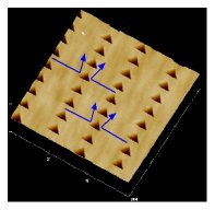
The first artificial nano-structured electronic material that functions at room temperature. One can cut a piece from the material and use it as an individual device. |
|
The nano-diode, called self-switching device, only requires only one instead of many steps of lithography. |
|
The simplest OR gate ever made, --by simply "writing lines" on a piece semiconductor. |
|
At nanometre scale, electrons actually behave like waves. This shows electron wave propagating through a narrow constriction (a so-called quantum point contact), at six consecutive moments. |
|
A parabolic reflector reflects electron waves out of a narrow constriction, about 30 nm wide. The fine fringes are due to the electron wave interference effect.
|
|
The wavelength of the electrons can be tuned very conveniently in semiconductor nanostructures. Electrons with two different wavelengths will propagate through a nanometre-scale constriction in completely different ways, as shown above (click to enlarge). It shows that at nanometre-scale, one has to treat electrons as waves rather than particles. This fascinating phenomenon was demonstrated in our simulations by solving an electron wave equation. Another interesting effect is that electron waves can "squeeze" into the narrow gap nearly perfectly, with very little reflectance, which is called adiabatic transport. |
||


We always welcome applicants who wish to carry out advanced research leading to a Ph.D. degree on semiconductor devices and nanotechnology. These posters (in PDF format) for the recent postgraduate open day contain examples of Ph.D. projects, which are most appropriate for students with a 1st or 2i honours degree in physics or electronics.