Nanometre-Scale Patterning
Conventional semiconductor devices are made using the
so-called photo-lithography. The resolution is typically 1 micron, limited by
the wavelength of the UV light used. To create nanometre-scale structures, electron beams have been used
to replace UV light in the so-called electron-beam lithography. The electrons
are accelerated by a very high voltage, typically tens of kV, and then focused
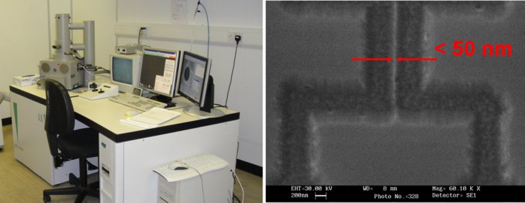
onto a layer of polymer to create very fine patterns. A photo of our
electron-beam lithography is shown below together with a fine nanochannel structure
that we fabricated with a linewidth below 50 nm.
Apart from the electron-beam lithography,
over the recent years, scanning probe microscope (SPM)-based nanotechnology has become a
very promising and competitive alternative to the electron-beam lithography.
SPM-based lithography consists two
approaches, mechanical and electrochemical. The mechanical approach is to use
the probe to plough or to perform probe indentation (tip oscillating) on the
surface of a thin layer of polymer on a semiconductor sample, in a very
accurate and well-controllable manner. Subsequent etch, for example, will be
carried out to transfer the nanometre-pattern to the semiconductor. The
electrochemical approach, based on local anodic oxidation (LAO), has become the
most popular method, in which the probe is negatively biased to impose a huge
local electric field of about 109 V/m and
hence induce a localized oxide beneath the probe. The oxidised areas typically
have an increased volume, and can be imaged conveniently using the AFM
immediately after the oxidation.
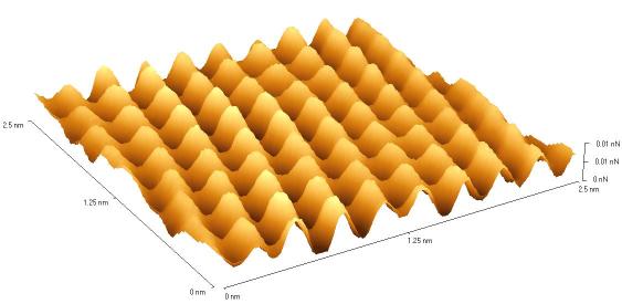
Our advanced CP-R SPM system has been a great tool for us to develop new types of semiconductor device concepts. Below are images showing the atomic resolution of our SPM and some of the patterns created.
|
|
|
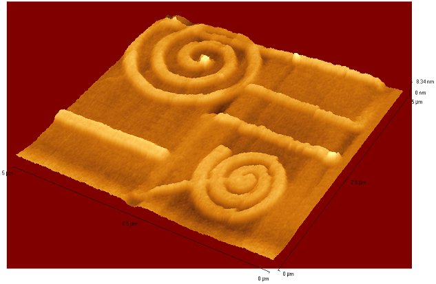
Spirals and lines created with our SPM on doped silicon substrate. |
|
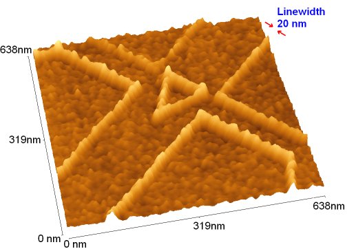
Pattern of a nanometre-scale ballistic rectifier created by anodic local oxidation. The Ti metal grains can also be clearly seen in the background.
|
|
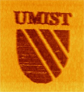
The UMIST logo shown here was made by our AFM recently on a piece of silicon. It is actually thousands times smaller than it appears!
|