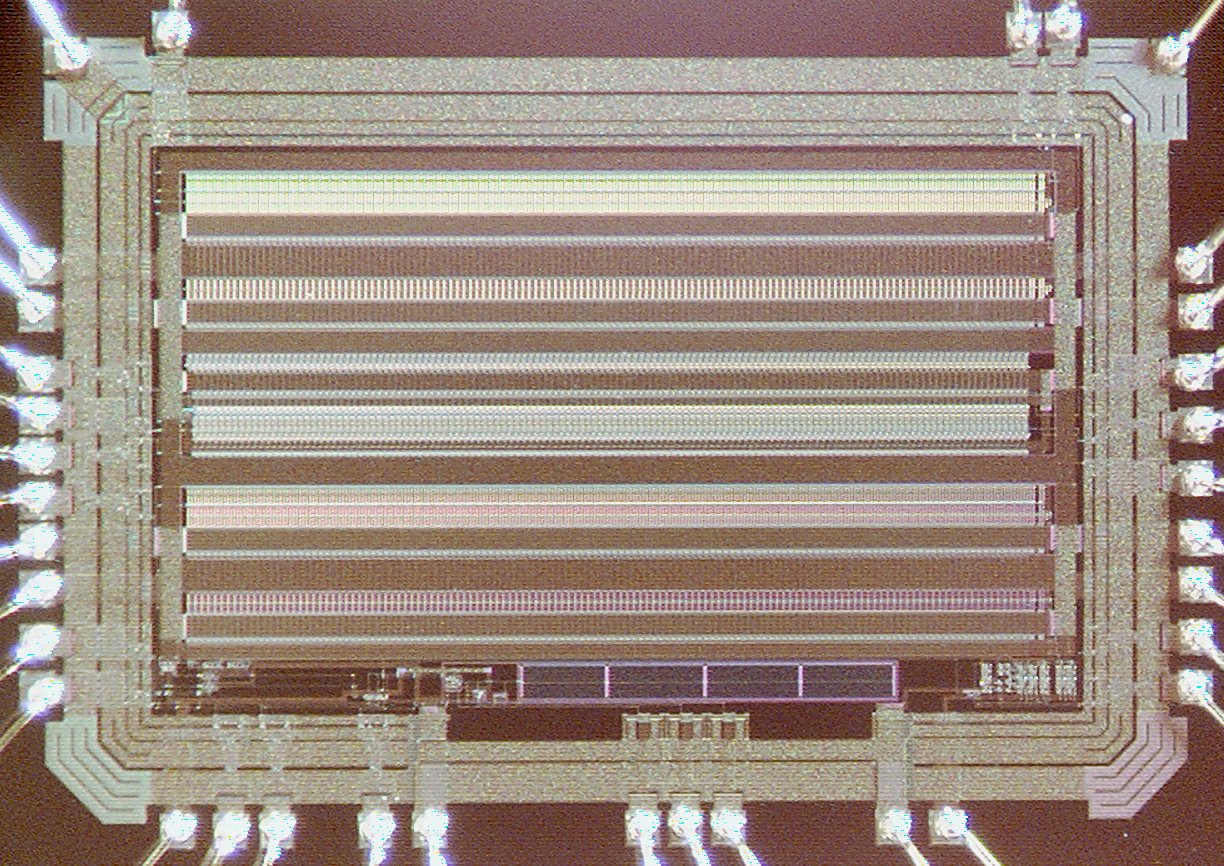
 chip photo (365kB)
 chip photo (365kB)
High resolution time-to-digital converters (TDCs) have application in a number of measurement systems, e.g. time-of-flight particle detectors, laser range-finders and logic analysers. Modern time-of-flight spectrometry systems, used in particle physics experiments as well as in industrial methods of material surface analysis require a TDC to have a resolution well below 1ns, low dead-time, and a large dynamic range. The VDL Time to Digital Converter chip utilises the vernier delay line (VDL) technique, which allows the achievement of these goals.
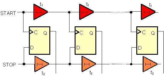
The operation of the VDL is based on the delay line method, where the time resolution is determined by a logic buffer delay. In the VDL two delay buffer chains are used. The delay of a buffer in the upper delay chain is slightly greater than the delay of a buffer in the lower delay chain. As the START and STOP pulses propagate in their respective delay chains, the time difference between them is decreased in each vernier stage by the difference in buffer delays. In each stage the signals are fed into an arbiter circuit (a D-type latch can perform this function) which decides which of the two pulses came first. The position in the delay line, at which the STOP signal catches up with the START signal, gives information about the measured time between START and STOP, with the resolution equal to the difference in buffer delays.
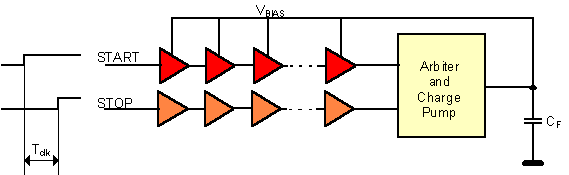
To stabilise the value of buffer delays against temperature or power supply voltage changes, and to calibrate chips against process variations the Delay Locked Loop (DLL) scheme is used. To allow the calibration of the delay a voltage-controlled delay buffers are used in the upper delay chain. The control voltage is adjusted by a feedback loop, which includes the VDL, an arbiter circuit, a charge pump, and a filter capacitor.
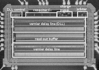
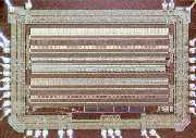
The integrated circuit that was fabricated in 0.7um digital CMOS technology. It consists of two 128-stage VDLs (one for measurements and one for the DLL), complete DLL circuitry, and a simplified parallel-input/serial-output read-out circuitry. The chip is a full-custom design, comprising over 10000 transistors. Total chip area is 3.2mmx3.1mm.
The TDC chip works with overall accuracy better than +/-1 LSB for resolutions down to 60 ps, stabilised in the continuously working DLL loop or for resolutions down to 30 ps when the DLL loop is used intermittently to stabilise the delay between measurements, or in averaging mode. DLL locks for resolutions in a range of 30 to 250ps. Alternatively, with external biasing, the VDL can achieve resolutions as high as 5 ps, however, the accuracy will be limited by the systematic non-linearity error and by the random error of 10ps caused by the time-jitter.
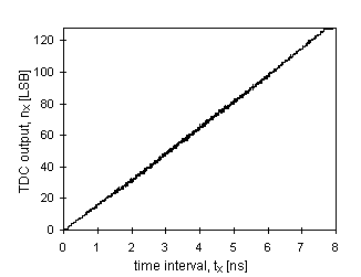
(Above) Measured single-shot TDC characteristics for the resolution of 60ps stabilised in the continuously working DLL. Random noise of 45ps rms which appears on the characteristics can be supressed by averaging.
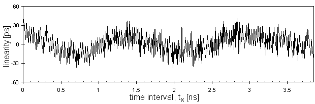
(Above) Measured integral non-linearity of the TDC characteristics for the resolution of 30ps and the DLL turned off. Maximum integral non-linearity is equal to 30ps. A random error of single-shot measurement is equal to 20ps rms.
References:
P. Dudek, S. Szczepanski and J.V. Hatfield, "A High-Resolution CMOS Time to Digital Converter Utilising a Vernier Delay Line", IEEE Journal of Solid State Circuits, vol.35, no.2, pp. 240- 247, February 2000
P. Dudek and J.V. Hatfield, "A Zero Dead-Time, High Temporal Resolution, Time-of-Flight Particle Detector IC", Proceedings of the Eurosensors XI Conference, Warsaw, Poland, pp. 1341-1344, September 1997