 chip
photo (223kB)
chip
photo (223kB) chip
photo (223kB)
Analogue integrated circuits can offer advantages over their digital counterparts, in terms of speed, power dissipation and silicon area consumed by the circuitry. However digital circuits are often a preferred solution in cases where programmability is required. The analogue microprocessor (AuP) effectively executes software programs, in a way akin to a digital microprocessor, while operating on analogue data samples. This enables the design of mixed-mode systems which retain the speed/area/power advantages of the analogue signal processing paradigm while being fully programmable, general-purpose systems.
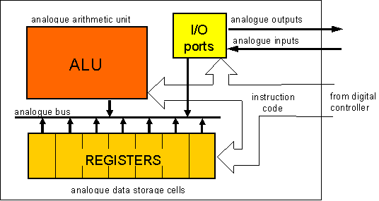
The AuP consists of a register file (each register is an analogue memory cell, capable of storing a sample of data), an analogue ALU (Arithmetic Logic Unit), and an analogue I/O port. All the building blocks are interconnected via an analogue data bus. The processing of information is performed entirely on analogue values. The AuP executes a software program, performing consecutive instructions issued by a digital controller. These instructions may include register transfer operations, which move the analogue samples of data between registers of the AuP, I/O operations which move the data to and from I/O ports, arithmetic operations, which modify the analogue data, and comparison operations, which allow for conditional branching. The program is stored in the local memory of the controller, which is a purely digital device. The complete processor is therefore a mixed-mode system, with an analogue data-path and a digital control-path.
The AuP is implemented utilising switched-current (SI) techniques. The simple structure of SI cells results in area- and power-efficient AuP implementations while offering adequate speed and accuracy to satisfy a wide range of applications. The register file is build using SI memory cells, which remember current by storing charge on a gate capacitance of a MOS transistor. The ALU needs only to explicitly implement multiplication, since the inversion operation is inherent in the SI memory, and the addition operation is performed with no area overhead on the analogue bus, using current summation. The multiplication is implemented using binary-scaled current mirrors.
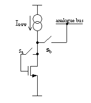 Basic switched-current memory cell.
The clock-feedthrough errors in SI memory cells will cause the AuP instructions to be performed with a limited accuracy. Signal-independent error compensation can be obtained by appropriate sequencing of the machine instructions. Several circuit techniques of signal-dependent error compensation (dummy-switches, S2I compensation etc.) were tested on the prototype chip. The more sophisticated methods of error compensation in SI cells require more complex circuitry, and therefore the design of an AuP will involves trade-offs between accuracy, speed, area and power. Our implementation of the AuP is targeted at a processor array, intended for low-level image processing. For this application, the primary consideration is the silicon area occupied by a single processor and power consumption. On the other hand a moderate level of accuracy is adequate for most low-level vision tasks.
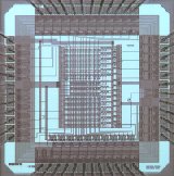
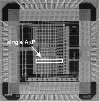
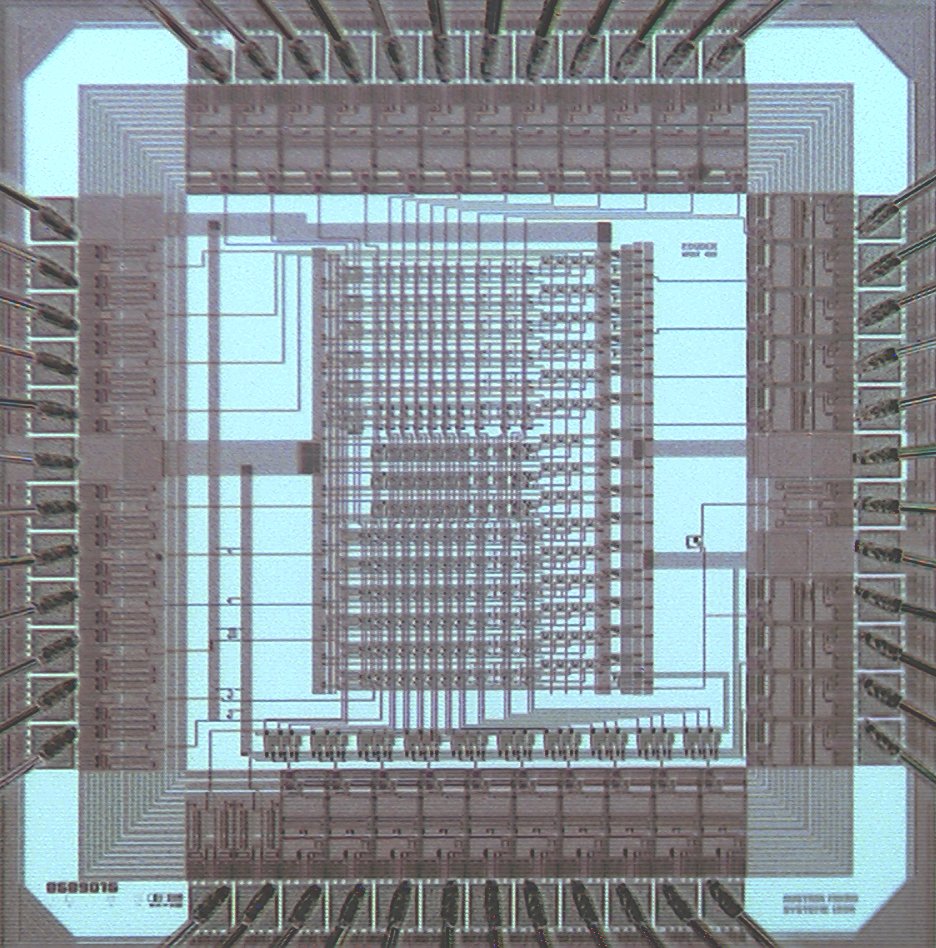
The prototype chip, fabricated in 0.8 um CMOS technology, contains 15 AuPs. The picture below shows in a box one of the processors, built using the S2I error compensation technique. The processor works with a clock frequency of up to 2.5 MHz. The total power dissipation within the processor is less than 100 uW. The effective area occupied by the processor, comprising six registers and a 3-bit multiplier, is equal to 11200 um2. As the typical assignment or arithmetic operation will take two clock cycles, the performance/area ratio for this processor is equal to 0.11 GOPS/mm2. (Giga Operations Per Second per mm2) The performance/power ratio is equal to 12.5 GOPS/W. These figures of merit compare quite favourably with those of digital processors, even simple bit-serial ones.
 Download 1024x1024 chip photo (223kB)
The maximum magnitude of the signal-dependent error, measured for a register transfer instruction, is equal to 2.5 %. Random errors are equal to 0.4 % per transfer. The analogue value held in the register decays due to the leakage currents at a rate of 0.5 % per 100 ms. Many applications, particularly in low-level image processing, are not very sensitive to the errors introduced by the AuP. As an example, consider the edge detection problem. A software for the AuP, implementing the Sobel edge detection algorithm has been written, and executed on the S2I processor. The processing results are presented below.
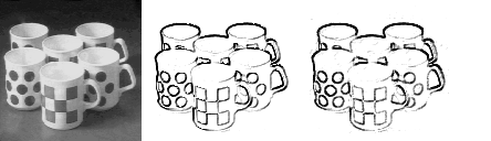
Original image (left,) results of ideal sobel edge detection (centre) and results of processing on the AuP (right)
The analogue microprocessor executes software programs while operating on analogue data values. The AuP paradigm will find application in areas that can benefit from employing analogue signal processing techniques, but where nevertheless the flexibility of a software-programmable device is needed. Small cell size and low power dissipation are the key features that enable massive parallelism. A very high performance system could be built by integrating a large number of processors. An SIMD array of 128x128 such AuPs could be feasibly accommodated on a single die and, when clocked at 2.5MHz, perform algorithms with a speed of over 20 GOPS while dissipating less than 2W of power.